
If this is the future of quantum computers and most modern control electronics are based on popular complementary metal-oxide-semiconductor (CMOS) technology, such scaling is a must. Therefore, such a future is highly demand driven.
This should not be overemphasized. From the first design and imprinted any indestructible silicon chip in wearing all patterns, it was rather clear, that none shall extend its dimensional, geometric projections carefully: very vague for example modern npn or pnp bipolar transistors.
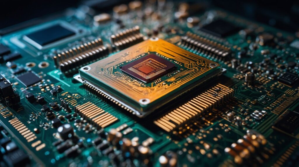
CMOS as architecture is not where the developments lie, but the application and possible seams at which the Conventional Power Electronics will meet with the level of processes now present in almost every day computing appliances, like portable mobile phones.
Without the means to produce these qubits in large quantity and low cost, there is little hope for quantum computers capable of performing useful calculations.
The Imec team took a completely different approach to this problem by using traditional methods in the construction of superconducting qubits already third phase on 300 mm silicon wafers. Such wafers are also used to produce advanced micro circuitry.
Key achievements include:
- High yield: 98.25% of the ungapped sourced, masu shaped qubits were functional.
- Long coherence times: Relaxation time T1 and coherence time T2 being greater than 100 micro sec.
- Scalability: This technique is amenable to use with the standard industrial semiconductor fabrication processes.
- Consistency: Provided evidence of similar characteristics across the wafer.
How They Did It
The qubit structures, especially the Josephson junctions, were fabricated by the researchers employing optical lithography and reactive-ion etching. This technique is different from the shadow evaporation technique most labs employ in most cases. Taking advantage of the industrial methods used, they obtained better control over the parameters of the qubit and even showed the room for better tuning.
Implications for Quantum Computing This work represents a significant step towards the practical realization of large scale quantum processors. On proving that good quality qubits are manufactured through industrial processes,
the work is a stepping stone to:
- Increased production volume: The existing semiconductor fabs may perhaps provide the much-needed quantum chips in large volumes
- Better uniformity and yield: Due to the industrial processes, there is a tighter and consistent control over the outcomes.
- Integration with classical electronics: Since the control and readout circuitry is CMOS compatible, the integration is less difficult
- Cost reduction: The use of available facilities may help reduce the costs involved in fabricating quantum hardware
Looking Ahead While this constitutes an important achievement as well, there are processes yet to be completed. The researchers pinpointed problem areas to be addressed, namely:
- Optimizing the oxidation process to promote even distribution of qubit frequency detuning
- Improving lithography control over the dimension of Josephson junctions so that size variation is mitigated
- Investigating three-dimensional integration techniques to aid in the fabrication of complex quantum circuits
Conclusion
This breakthrough demonstrates that the quantum computing industry is maturing and is ready to incorporate standard processes known in the semiconductor manufacturing industry. As these processes get perfected and adopted one could expect even faster growth in developing even more extensive and more powerful quantum processors.
Implications for Quantum Computing This work represents a significant step towards the practical realization of large scale quantum processors. The objective in this research is to achieve the stated objective by demonstrating that it is possible to:
- To ramp up guarantees high-volume production: The existing semiconductor fabs may perhaps provide the much needed quantum chips in large volumes.
- Taking control yields results: As a result of these industrial processes, there is a tight and consistent control over the outcomes.
- Suitable materials and devices: Since the control and read out circuitry is CMOS compatible, integration is less difficult
- Cost saving: The existing facilities may help cut down on the expenses involved in the fabrication of quantum hardware facilities
Looking Ahead
This however constitutes an important achievement as well, unfortunate processes, however, processes are yet to be completed. The researchers pinpointed problem areas to be addressed by researchers namely:
- Reducing the degree of randomness in the distribution of qubit frequency detuning via optimization of the oxidation process.
- Improving l17iconographicrol over the dimension of Josephson junctions so that sizal98e variations are being mitigated.
- Searching for three dimensional integration methods for the implementation of more advanced quantum circuits.