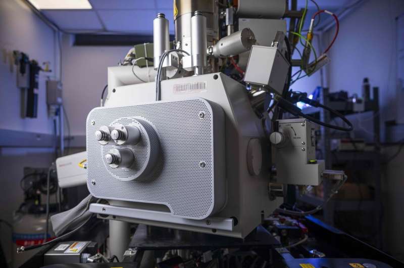
Researchers at UC Santa Barbara have achieved a groundbreaking feat – capturing the first-ever “movie” of electric charges traveling across the interface of two different semiconductor materials. This revolutionary imaging technique, known as scanning ultrafast electron microscopy (SUEM), allows scientists to directly observe the fleeting phenomenon of photocarrier movement, which is crucial for understanding and optimizing semiconductor devices like solar cells and lasers. The research, published in the Proceedings of the National Academy of Sciences, showcases the potential of SUEM to transform our understanding of semiconductor physics and device performance.
Visualizing Hot Photocarrier Transfer at Semiconductor Heterojunctions
The ability to visualize the movement of photoexcited charges, or “photocarriers,” across the interface of two different semiconductor materials, known as a heterojunction, is a game-changer in the field of semiconductor research. Traditionally, scientists have relied on theoretical models and indirect measurements to understand this process, which is critical for the performance of a wide range of electronic devices, from solar cells to lasers.
Led by Associate Professor Bolin Liao, the research team at UC Santa Barbara has developed the SUEM technique to directly observe these fleeting photocarrier dynamics. The key to their imaging approach is the use of ultrafast laser pulses, which act as a picosecond-scale shutter, allowing them to capture the movement of hot photocarriers as they diffuse across the junction between silicon and germanium, two common semiconductor materials.
Shedding Light on Charge Trapping and Device Performance
The researchers’ findings provide valuable insights into the behavior of hot photocarriers at semiconductor heterojunctions. They observed that when charges are excited near the junction, a fraction of them become trapped by the junction potential, slowing down their movement. This charge trapping phenomenon, which can negatively impact the performance of devices that rely on separating and collecting hot charges, has long been understood in semiconductor theory, but had never before been directly visualized.
According to Liao, “We didn’t expect to be able to image this effect directly. This paper is really about demonstrating the capability of SUEM to, for example, study realistic devices.” The ability to see how hot photocarriers behave at heterojunctions can help semiconductor device designers address potential performance challenges and optimize the design of their technologies.
The research also connects back to the pioneering work of the late UC Santa Barbara engineering professor Herb Kroemer, who in 1957 first proposed the concept of semiconductor heterostructures, laying the foundation for modern microchips, computers, and information technology. Kroemer’s idea that “the interface is the device” has become a fundamental principle in the field, and the new SUEM visualizations bring this concept to life.
By directly observing the movement of hot photocarriers across semiconductor heterojunctions, the UC Santa Barbara team has taken a significant step forward in understanding the fundamental processes that underpin a wide range of electronic and optoelectronic devices. This knowledge can inform the design and optimization of solar cells, lasers, sensors, and other technologies that rely on the efficient management of charge carriers.
Harnessing the Power of Hot Photocarriers for Energy Efficiency
The research has broader implications for improving the energy efficiency of semiconductor devices. When sunlight hits a semiconductor material, it excites electrons, creating electron-hole pairs known as photocarriers. These photocarriers can then be harnessed to generate electricity in solar cells or drive other electronic processes.
However, these hot photocarriers typically lose most of their energy within picoseconds, or trillionths of a second, before they can be put to use. Conventional photovoltaic technologies can only harvest a fraction of the energy these carriers have in their “hot” state, with the rest being released as waste heat.
Understanding how hot photocarriers behave at semiconductor heterojunctions, as revealed by the SUEM visualizations, could pave the way for new strategies to better harness their energy. By optimizing the design of semiconductor devices to capture and utilize these hot carriers more effectively, it may be possible to significantly improve the efficiency and performance of technologies like solar cells, potentially leading to breakthroughs in renewable energy and beyond.