Now, it is leading the way for making miniaturized electronics and computing devices using a millennia old luxury product/silk. So the team put a two-dimensional (2D) silk protein on graphene to create bio-electronics.
Taming the Silk Tangle
Silk has been a part of the trade history for centuries now due to its special features- elasticity, tensile strength and durability. But silk has a bad habit of getting tangled up in a messy mass of silk fibers, which has prohibited the material from being used much for designer electronics.
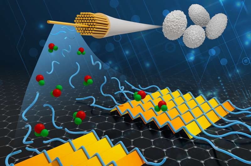
But they just might have an ally in taming the tangle, thanks to a team of researchers at Pacific Northwest National Laboratory. They were able to produce a consistent monolayer of silk protein fragments (or fibroins) on the graphene –a carbon-based material with great electrical conductivity. The discovery is a key step to addressing how silk protein self-assembles, an important result that will allow for all-silk electronics to be designed and fabricated in the first instance.
The researchers note that this non-toxic, water-based system is essential for the biocompatibility of their technology. This material combination of silk on graphene has great potential as it provides a sensitive, tunable transistor which operates at very low voltages; the holy grail for developing implantable and wearable health sensors.
Potential uses of silk in neural networks
The PNNL team expects this silk-on-graphene system to ultimately form the basis of memory transistors or ‘memristors’ in computing neural networks. The third layer of our approximation started to congeal in the late 2000s with experimental advances producing the first verifiably working memristors—components capable of mimicking human brain nerve cells and are used in all neural networks.
‘Lots of research has been done using silk as a substrate for controlling electronic signals, but because silk proteins are by nature disordered, only basic modulation has been achieved,’ says James De Yoreo, Battelle Fellow at PNNL and Professor in the Materials Science & Engineering and Chemistry departments at University of Washington. With the knowledge we had in controlling material growth on surfaces, we were like ‘can we develop an even better interface?’ ‘.
By tuning the reaction conditions and slowly adding individual silk fibers into water-rich system in a controlled way, they have been able to create an ordered 2D layer of proteins with tight packing in precise parallel β-sheets — one of the most common protein conformations found. This organized structure at the nanoscale enables miniaturization, in line with trends demanded by biological-electronics applications, and therefore a promising basis for neural networks and more advanced computing purposes.
Conclusion
The 2D silk protein layer presents a major technical breakthrough in the integration of silk-based materials for applications in microelectronics and computing. This eco-friendly yet effective methodology, which can be adapted to improve the stability and conductivity of silk-embedded circuits or expand the application scope of silk in biodegradable electronics, will pave a promising way for future green and sustainable implementation in this sector. More work needs to be done, but the ultimate goal of these researchers is to expand their technology to reach new heights in computing and wearable/ingestible health solutions.