Researchers at the Oak Ridge National Laboratory have developed a groundbreaking technique called RODAS (Rapid Object Detection and Action System) that enables the observation of atomic-level changes in materials, paving the way for advancements in quantum computing and electronics. This technique combines imaging, spectroscopy, and microscopy methods to capture the properties of fleeting atomic structures as they form, providing unprecedented insights. Quantum computing and quantum electronics stand to benefit greatly from this innovation.
Evolving Material Characterization via RODAS
The RODAS technique is a major advance in materials science. This allows researchers to interactively probe structure-property relationships as the analysis proceeds, select and optically track specific atoms or defects for measurement as they form, efficiently gather data on many types of defect simultaneously, respond to identify new atomic or defect classes in real-time and minimize damage to the sample while preserving fine structural detail.
Traditional approaches utilizing scanning transmission electron microscopy (STEM) in combination with electron energy loss spectroscopy (EELS), are restricted by the ability of the high-energy charged particle beam to alter or degrade the specimen during analysis. RODAS does so by augmenting the system with dynamic computer-vision-enabled imaging that continuously learns and focuses only on the subjects of interest in real-time. It allows for extremely fast analysis, requiring only seconds or milliseconds compared to the many minutes necessary in other STEM-EELS methods. And, it is non-destructive to the sample, unlike most techniques.
Defect Probing and Quantum Materials Secrets
Materials are not perfect, and imperfections – defects – in materials can directly affect any of the vast range of properties exhibited by a material be they electronic, mechanical, or quantum. Defect structures can be arranged intrinsically in different ways at the atomic scale but also under the influence of external excitation such as electron beam irradiation. These defect configurations hold the key to discovering tomorrow’s materials for quantum computing and electronics.
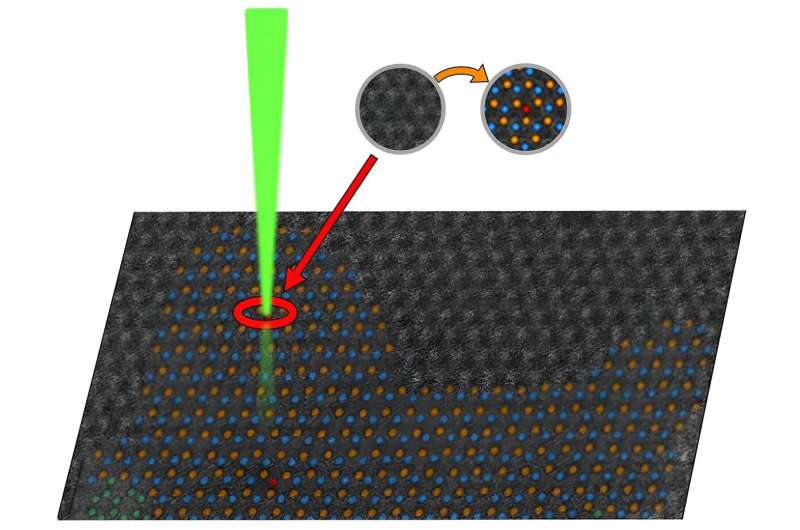
For example, the research team showed the RODAS technique on a single layer of molybdenum disulfide, which is a popular semiconductor material for applications like quantum computing and optics. Molybdenum disulfide is already considered one of the most promising candidates in its class, largely because it can produce single photons from defects (specifically single sulfur vacancies). One possibility for single-layer materials, such as molybdenum disulfide, is that the optical or electronic properties of the material change drastically at atomic scales.
Iconic Examples of Materials and Technology Progress
From the perspective of materials science, the RODAS technique presents unprecedented opportunities for tracking and analyzing materials on an atomic level in real-time. It lets you explore and characterize materials in motion — great for understanding how materials respond to different stimuli.
“Materials science methods like advanced electron microscopy are giving us more direct knowledge about the physical world, and systems like RODAS could help propel discovery and innovation,” said lead author Kevin Roccapriore from ORNL’s Center for Nanophase Materials Sciences. Berei also predicted that “The ability to study materials in real-time at the atomic scale has the potential to change how we develop new materials, pushing frontiers in computing and electronics (and beyond) — even allowing us to make Feynman’s dream of shrinking machines smaller and more efficient.